

Digital Gauge Frequently Asked Questions
Question number FAQ-0063
Description of the DG-4240 BCD OUT connector signal
For details, please refer to the instruction manual.
To capture BCD signals into a sequencer or similar device, please ensure to hold the signal with a hold signal.
For connection with external devices, please refer to DG4240 BCD receiving side recommended circuit.
(1) BCDout connector, cable
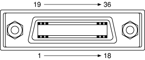
AA8107 type BCD signal code 3m ¥12,000
One side with the above connector, one side open, length 3m
Available as an option.
- Compatible connector type
Receptacle: DX10A-36S (Hirose Electric)
Compatible plug: DX40-36P (Hirose Electric)
Plug cover: DX36-CV1 (Hirose Electric)
- Cable specifications
Wire size ;AWG #30
Conductor configuration ;7/0.1
Wire outer diameter ;φ0.5
Cable UL style;UL20276 and UL2789
(2) BCD connector pin numbers and signal content
| PIN number | signal content | PIN number | signal content |
|---|---|---|---|
| 1 2 3 4 |
1×10 0 BCD output 2×10 0 4×10 0 8×10 0 |
19 20 21 22 |
4×10 4 8×10 4 LOWER output OK output |
| 5 6 7 8 |
1×101 2×101 4×101 8×101 |
23 24 25 26 |
UPPER output N.C Polarity output + Polarity output - |
| 9 10 11 12 |
1×10² 2×10² 4×10² 8×10² |
27 28 29 30 |
D.P3 decimal output[10μm, 0.00] D.P4 decimal output[1μm, 0.000] N.C Error output |
| 13 14 15 16 |
1×10³ 2×10³ 4×10³ 8×10³ |
31 32 33 34 |
Hold output Reset input BUSY input Compare gate input |
| 17 18 |
1×10⁴ 2×10⁴ |
35 36 |
Print command output common |
Explanation of signal content
- BCD output Pin No. 1-20
Positive/Negative logic switch 5-digit parallel output
Open collector output
The bit switch 3 below <18> can be switched to negative logic when on and to positive logic when off.
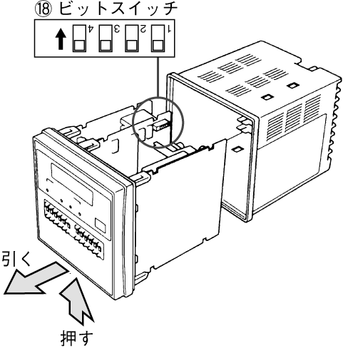
- Pass/Fail Judgment Output
Pin No. 21 (LOWER output) ON when LOWER setting value ≧ count value
Pin No. 22 (OK output) ON when LOWER setting value < count value < UPPER setting value
Pin No. 23 (UPPER output) ON when UPPER setting value ≧ count value
Open collector output
- Polarity output Pin No.25 (+ output), No.26 (- output)
Open collector output
- Set Bit Switch 3 to on, and if selecting negative logic:
When the measurement is positive (+): No.25: on (Low level), No.26: off (Hi level)
When the measurement is negative (-): No.25: off (Hi level), No.26: on (Low level)
During reset: No.25: on (Low level), No.26: off (Hi level) - When Bit Switch 3 is turned off and positive logic is selected, the on/off states for items No. 25 and 26 above will be reversed.
- Decimal Point Output
Pin No. 27 (D.P3, minimum measurement unit 10μm selected)
Pin No. 28 (D.P4, minimum measurement unit 1μm selected)
Open Collector Output
- When bit switch 3 is turned on and negative logic is selected,
if bit switch 1 is turned on and 1μm is selected: No.27: off (Hi level), No.28: on (Low level)
If bit switch 1 is turned off and 10μm is selected: No.27: off (Hi level), No.28: on (Low level) - If you turn off bit switch 3 and select positive logic, the on/off states for items 27 and 28 above will be reversed.
- Error Output Pin No. 30
Open collector output
If a miscount occurs in the counting circuit of this device, an on signal will be output.
The on signal will continue until it is reset.
- Hold Input Pin No. 31
When a Lo level voltage signal is input, the displayed value and BCD output data are held, and a print command signal is output. This signal maintains the hold state while it is at Lo level. However, even during the hold state, the counting circuit internally continues to perform counting operations based on the input signal from the gauge sensor, so when the hold is released, the displayed value and BCD output data will change to the measurement value at that moment.
- Reset Input Pin No. 32
When a low-level voltage signal is input, the displayed value, BCD output data, error display, and error output are reset. The reset state will continue while this signal is at a low level.
- BUSY input Pin No. 33
It is in the same state as the hold input. It is used for timing of external devices such as printers.
- Comparator Gate Output Pin No. 34
When a low-level voltage signal is input, the pass/fail judgment is forcibly stopped, and all pass/fail judgment outputs are turned off.
- Print command output Pin No. 35
Open collector output
When the hold signal or BUSY signal is input, and the displayed value and BCD output enter the hold state, a negative pulse print command signal is output.
Last updated: 2000-12-08